Lonten Tech
Custom C8051F020 F120 F040 Small System Learning and Development Board Core Board
Custom C8051F020 F120 F040 Small System Learning and Development Board Core Board
Couldn't load pickup availability
Main features of the development board:
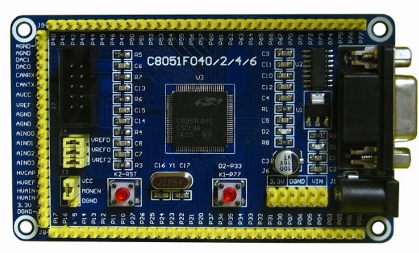
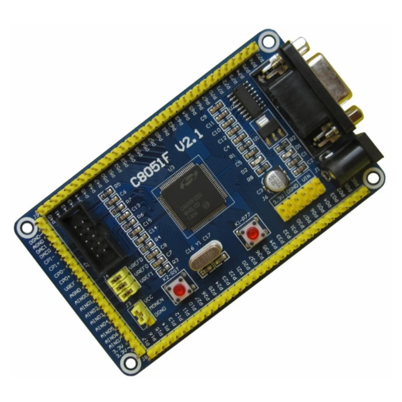
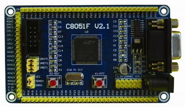
The appearance design of the product is exquisite, from the design of the schematic to the completion of the PCB, everything is based on the principle of continuous improvement. Reasonable component layout, standardized and precise manual wiring are incomparable to the software's built-in automatic wiring, in order to further improve the performance of the product
The SMT components are produced by machine reflow soldering
The pins for pin expansion are all led out with a standard 2.54mm spacing and clearly labeled. The arrangement of each port has been optimized for more convenient use. The spacing between the two rows of pins for pin expansion is designed according to the commonly used spacing of a universal board. Therefore, if you want to insert this system board into a hole board, simply install and weld the pins facing downwards
◆ The default shipment is suitable for external circuits with DuPont wires soldered with the pins facing upwards. If you need to solder with the pins facing downwards or do not solder the pins, please indicate when purchasing.
Shipping list:
◆ One development board
◆ One USB power cable
4 circuit board pillars
◆ One data CD
(The CD contains: example programs, development software, circuit diagrams, chip manuals, and a large number of reference learning materials)
Introduction to internal resources of C8051F020 chip:
C8051F020 8051 compatible CIP-51 core with high-speed pipeline structure
Full speed non-invasive system debugging interface (on chip)
A true 12 bit 100ksps 8-channel ADC with PGA and analog multiplexer switch;
8-bit 500ksps 8-channel ADC
Two 12 bit DACs with programmable update timing
64K bytes of programmable FLASH memory in the system
4352 (4096+256) bytes of on-chip RAM
External data storage interface with an addressable 64K byte address space
Hardware implementation of SPI, SMBus/IIC, and two UART serial interfaces
5 universal 16 bit timers
Programmable counter/timer array with 5 capture/comparison modules
On chip watchdog timer, 2 comparators, VDD monitor, and temperature sensor
64 I/O ports
-Industrial grade temperature range of 40~85 degrees Celsius
2.7V~3.6V working voltage, 100 pin TQFP package
Introduction to internal resources of C8051F120 chip:
High speed, pipelined 8051 compatible CIP-51 core (100MIPS or 50MIPS)
Full speed, non-invasive system debugging interface (on chip)
True 12 or 10 bit, 100 ksps ADC with PGA and 8-channel analog multiplexer switch
A true 8-bit 500 ksps ADC with PGA and 8-channel analog multiplexer switch (C8051F12x only)
Two 12 bit DACs with programmable data update mode (C8051F12x only)
2-cycle 16 x 16 multiplication and accumulation engine (C8051F120/1/2/3 and C8051F130/1/2/3 only)
128KB or 64KB FLASH memory that can be programmed in the system
8448 (8K+256) bytes of on-chip RAM
External data storage interface with addressable 64KB address space
Hardware implementation of SPI, SMBus/I2C, and two UART serial interfaces
5 universal 16 bit timers
Programmable counter/timer array with 6 capture/compare modules
On chip watchdog timer, VDD monitor, and temperature sensor
Introduction to internal resources of C8051F040 chip:
(1) 8051 compatible CIP-51 core with high-speed pipeline structure, achieving a execution speed of 25MIPS;
(2) Full speed non-invasive system debugging interface (on chip, JTAG interface);
(3) A true 12 bit C8051F040 100 ksps 13 channel ADC with PGA programmable amplifier
Gain: 16, 8, 4, 2, 1, 0.5 and analog multiplexer switch
(4) Two 12 bit DAC converters
(5) High precision programmable 24.5MHz internal oscillator;
(6) 64KB bytes of FLASH memory that can be programmed in the system;
(7) 4352 (4096+256) bytes of on-chip RAM;
(8) Hardware implementation of SPI, SMBus/IIC, and 2 UART serial interfaces;
(9) 5 universal 16 bit timers;
(10) Programmable counter/timer array with 6 capture/comparison modules;
(11) On chip power on reset, watchdog timer, 3 voltage comparators, VDD monitor and temperature
Sensors;
(12) 64 I/O ports;
(13) -40~85 degrees industrial temperature range;
(14) 2.7V~3.6V working voltage, packaged in TQFP100;


Share


